-
Mail us
contact@tiger-transformer.com -
Phone us
(+86)15655168738 -


Mail us
contact@tiger-transformer.comPhone us
(+86)15655168738
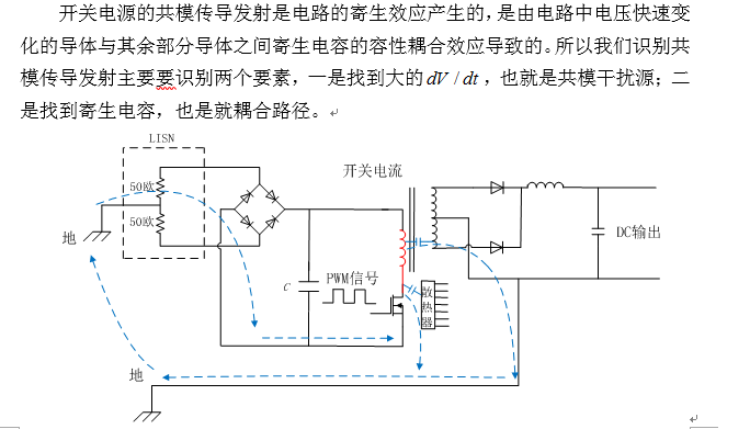
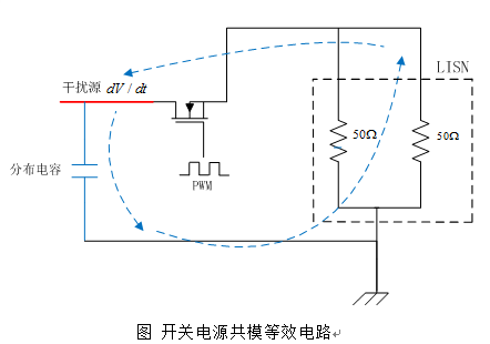
As can be seen from the above figure, the switching power supply is in the process of turning on and off the MOS tube. , the voltage of the primary side of the transformer and the part of the wire connecting the primary side of the transformer to the drain of the MOS tube is changing rapidly. This large part is the source of noise emitted by common mode conduction.
With the source of noise, let’s find the coupling path.
(1) Since the MOS tube switches on and off quickly, it will generate a lot of heat, so a radiator will be designed close to the MOS tube, but this will bring about a problem between the radiator and the MOS tube. There will be a large distributed capacitance between the drains, and the voltage at the drain is changing rapidly, thus generating a common-mode current from the drain to the heat sink.
(2) There is a large distributed capacitance between the primary side and the secondary side of the transformer, which generates a common mode current from the primary side to the secondary side. From the figure above we can see the return path of the common mode current. The switching tube's capacitance to the radiator constitutes the largest distributed capacitance, which is usually the main contribution path to common-mode conduction emissions.
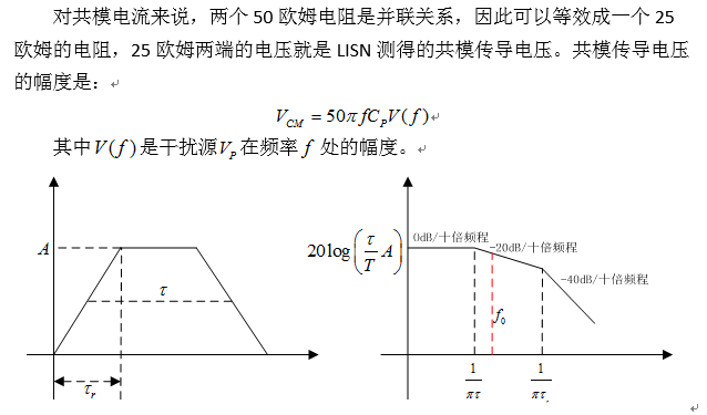
Next, we will theoretically analyze common-mode conducted emission. This analysis aims to improve everyone’s theoretical analysis ability of common-mode conducted emission. The actual model is more complicated than this, but we must first analyze this. a simplified model.