-
Mail us
contact@tiger-transformer.com -
Phone us
(+86)15655168738 -


Mail us
contact@tiger-transformer.comPhone us
(+86)15655168738
1. EMC characteristics of FLYBACK
The voltage oscillation peaks and current oscillation peaks formed by the switching power tube of FLYBACK (flyback converter) at the turn-on and turn-off moments are the main sources of interference in switching power supplies. , plays a decisive role in the conduction interference and radiation interference of the switching power supply. This article explains the switching spike formation process under CCM conditions.
2. Basic working principle of FLYBACK
(1) When the MOSFET is turned on, the input voltage charges the primary side of the transformer and the secondary side DIODE is cut off by the reverse voltage;
(2) When the MOSFET turns off, the energy stored on the primary side is transferred to the secondary side, causing DIODE to withstand the forward voltage drop and start to conduct, providing energy to the output load;
(3) At the moment when the switching power tube is turned on and off, a very high change rate of dv/dt and di/dt will be generated, which not only imposes high requirements on the voltage and current resistance of the tube, but also produces a very wide spectrum (the interference spectrum of the switching power supply is generally (below 200 MHz) electromagnetic interference;
(4) The factors affecting the switching waveform of the power switch tube of the actual flyback converter are relatively complex, and are not only affected by its own parasitic parameters, but also by external factors. interference;
3. Analysis of the switching process of FLYBACK under CCM
The following mainly analyzes the causes of the interference waveform under the influence of its own parasitic parameters.
3.1 FLYBACK circuit parasitic parameter characteristics
The actual operating waveform of FLYBACK is affected by factors such as PCB parasitic inductance, transformer leakage inductance, transformer parasitic capacitance, and the parasitic parameters of the device itself.
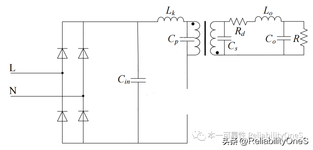
Figure 3-1 shows the schematic diagram of FLYBACK parasitic parameters. Among them, Cin and Co are the input and output capacitances, Lk is the leakage inductance of the transformer and the parasitic inductance of the PCB trace on the primary side, Cp and Cs are the parasitic capacitances of the primary and secondary windings of the transformer respectively, Cm and Cd are the parasitic capacitances of the switching tube, Lo It is the parasitic inductance of the secondary PCB trace and the secondary equivalent leakage inductance.
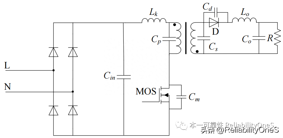
Figure 3-1 Parasitic parameters of flyback converter< /p>
3.2 Analysis of the turn-off process of MOS tube under CCM
3.2.1 Initial state in CCM mode
STEP1: The MOSFET tube is in the on state before T0, DIODE is in the cut-off state;
STEP2: The driving signal at T0 is low level, causing the MOSFET to enter the cut-off state from off;
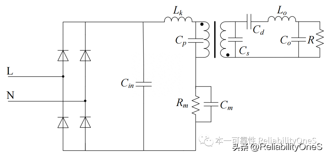
Note: Figure 3-2 shows the MOSFET tube at T0 Schematic diagram of the process from starting to turn off to ending. In the figure, Rm is the on-resistance of MOSFET, and Rd is the on-resistance of DIODE.
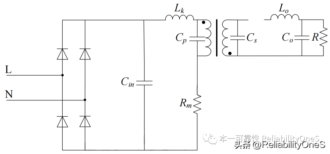
Figure 3-2 MOSFET is turned off at time T0 Schematic diagram of the deadline process - time before T0
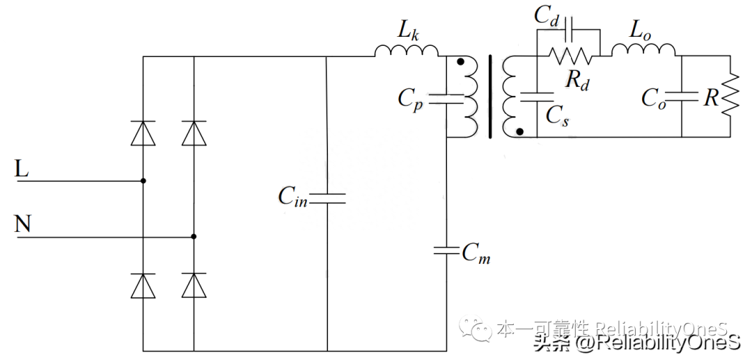
Figure 3- 2 Schematic diagram of the process from turn-off to cut-off of MOSFET at T0 moment - T0 turn-off moment
 < /p>
< /p>
Figure 3-2 Schematic diagram of the MOSFET process from turn-off to cut-off at time T0 - cut-off time after T0
3.2.2 MOSFET turn-off to cut-off process
STEP1: Before T0, the input terminal charges Lk, Cp, and Cin;
STEP2: When T0 is turned off, Lk, Cp, and Cin need to release energy. In the input loop and Cm, etc. The strong oscillating voltage and oscillating current of the LC are formed, superimposed on the voltage and current waveforms of the MOSFET, forming a large voltage peak oscillation and a large current peak oscillation. This is the moment when the MOSFET turns off during our actual waveform test. The reasons for voltage spike oscillation and current spike oscillation;
STEP3: At the cut-off moment, the energy release of Lk and Cp is zero, and the MOSFET tube is completely cut off;
3.2.3 DIODE is turned on to The conduction process
Due to the characteristics of FLYBACK, the processes of DIODE and MOSFET at T0 time are opposite.
STEP1: At the time before T0, DIODE is in the cut-off state and charges Cs;
STEP2: At T0, DIODE begins to conduct, and Cs begins to discharge and form with Cd, Lo, and Co LC oscillator circuit, but because the energy of Lo and Cd before T0 is zero and Cs is pF level, the stored energy is small, causing the LC circuit to form a small voltage spike oscillation and current spike oscillation. When this is the voltage and current we observe DIODE The reason for the relatively small voltage and current peak oscillation at the turn-on moment of the current;
STEP3: When the MOSFET is completely turned off, when the DIODE is completely turned on, Cd, Lo, Co, and Cs are charged.
3.3 Analysis of the turn-on process of MOS tube under CCM
3.3.1 Initial state in CCM mode
STEP1: The MOSFET tube before T1 is in the cut-off state, DIODE In the conduction state;
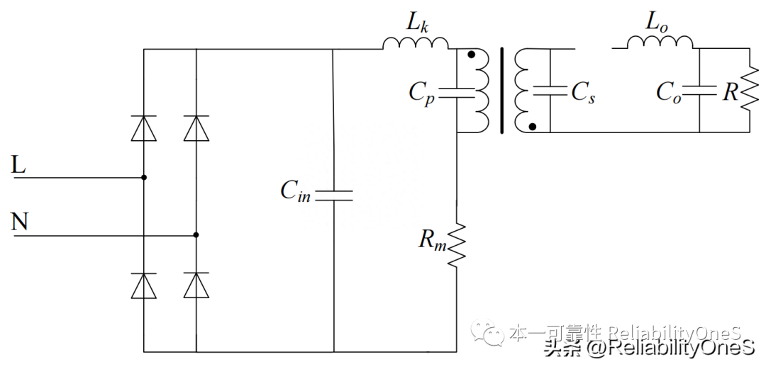
STEP2: The drive signal is high level at T1, causing the MOSFET to enter the conduction state from turn-on. Figure 3-3 is a schematic diagram of the MOSFET process from turn-on to conduction at T1;< /p>
Schematic diagram of the MOSFET process from turn-on to conduction at time T1- Time before T1
3.3.2 MOSFET turn-on to conduction process
The moment from turn-on to turn-on of MOSFET is correct It is the process of DIODE from off to cut off;
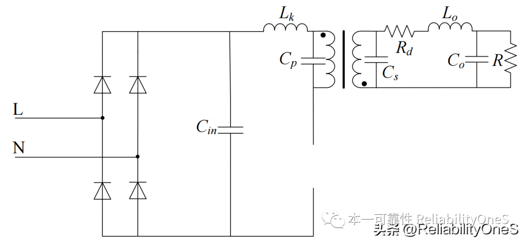
STEP1: When before T1, the output circuit charges Lo, Cs, Co, Cd;
STEP2: When T1 is on , Lo, Cs, Co, and Lo need to release energy, forming a strong oscillating voltage and oscillating current of LC in the output loop, which is superimposed on the voltage and current waveforms of DIODE, forming a larger voltage spike oscillation and a larger current spike. Oscillation, this is the reason why the DIODE tube has voltage peak oscillation and current peak oscillation at the turn-off moment during our actual waveform test;
STEP3: At the turn-on moment, the Cs and Lo energy release is zero, and the DIODE The tube is completely cut off.
3.3.3 DIODE’s turn-off to cut-off process
Due to the characteristics of FLYBACK, the process of DIODE and MOSFET at time T1 is opposite;
STEP1: When T1 At the moment before T1, the MOSFET is in the cut-off state and charges Cp;
STEP2: At the moment T1, the MOSFET begins to conduct, and Cp begins to discharge to form an LC oscillation loop with Cin, Lk, and Cm. However, due to the Lk, Cm before T1 The energy is zero and Cp is p. The stored energy of the F-level is small, causing the LC loop to form a small voltage spike oscillation and current spike oscillation. When we observe the voltage and current of the MOSFET tube, there is a relatively small amount at the turn-on moment. Causes of voltage and current spikes and oscillations;
STEP3: When the MOSFET is fully turned on, DIODE is completely turned off, and Cin, Lk, Cm, and Cp are charged;
4. Thoughts and Enlightenments
(1) The noise source of FLYBACK is dV/dt and di/dt formed by the power tube switch;
(2) The parasitic parameters of the power loop are the turn-on and The main cause of the turn-off spike should be avoided at the design end to reduce parasitic parameters;
(3) Analyze the turn-on and turn-off processes to better understand the characteristics of the noise source;