-
Mail us
contact@tiger-transformer.com -
Phone us
(+86)15655168738 -


Mail us
contact@tiger-transformer.comPhone us
(+86)15655168738
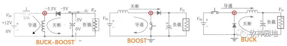
For switching power supply topology: inductor, switching tube The node between the diode and the diode is called the switching node; after the current flows into the node from the inductor, it can either flow out of the diode or the switch tube (depending on the switch tube state), so the current at the node flows alternately between the diode and the switch tube, maintaining a large current, and at the same time the node voltage must also fluctuate in a wide range (the voltage across the inductor jumps), and it can be seen that its voltage is chopping style. The figure below shows the BUCK-BOOST, BOOST and BUCK topologies, and the red circles are the switching nodes of each topology; taking the BUCK-BOOST topology as an example, the node voltage is +12V when the switch tube is turned on. , and the voltage at the node is -5.5V when the switch tube is "off", so the voltage waveform at this node is chopping in the range of 12V and -5.5V.
——An electric field antenna is naturally formed at the switching node (large voltage jump range and large current), which will cause radio frequency interference (EMI ), the output power supply voltage wire may receive the radiated interference and transmit it to the load end, causing noise interference.
As shown in the figure above, there are three basic types of switching power supply Topology, all other switching power supply topologies are based on the improvement and combination of these three topologies, but the working principle of switching topologies is the same; we only need to thoroughly grasp these three basic power supply topologies, other switching The power topology analysis will become simple:
As shown in the left figure below, the MOS tube in the red box replaces the freewheeling diode and becomes a synchronous BUCK power supply topology (the upper and lower MOS tubes need to be synchronized Design: One MOS tube is "off" while the other MOS tube is "on");
As shown in the figure on the right below, the inductor is replaced by a transformer to become a flyback topology, and at the same time There are push-pull, positive, half-bridge, full-bridge power topologies, etc.;
The BUCK, BOOST and BUCK-BOOST topologies can be cascaded in pairs to form new types of power topologies: Cuk, Sepic and Zeta topology etc.
The input-to-output conversion topology circuit of the power supply is composed of a series and parallel combination of switch tube + inductor + diode. There are n types (N> simply from the combinational logic) 10), then why are only these three effective power supply topologies?
I remember talking about the design issues of "common ground" and "floating ground" in the chapter "Resistor Application". Regardless of whether the ground is shared inside the board, it will eventually be connected to the "earth" and flow back to the "earth"; then why does everyone have to connect to the "earth"? Because the earth is an equipotential body, as long as all devices are connected to the "earth", the two devices share the same ground (grounding is not so simple, and will be analyzed in detail in the follow-up Electromagnetic Compatibility Basics grounding issues).
——The "ground" of the power grid system is the "earth", and all the power of the grid system needs to return to the "earth" after output.
Is it okay for the two devices to "float" each other? As long as there is no electrical contact (for example: connected with a fiber optic cable) it should be fine. But as long as there is electrical contact, there may be two problems:
Two signals with different reference ground systems cannot recognize and judge each other;
——Only for single-ended signals, differential signals will not be affected after ACcoupling (provided by the common mode level receiver);
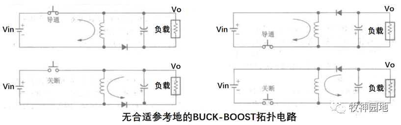
Speaking back to the power topology, except for the three basic topologies of BUCK, BOOST, and BUCK-BOOST, there is no common ground between the input and output of some topologies (for non-isolated topology, the power supply cannot return), that is, there is no suitable reference ground between the switching topology and the rest of the system. As shown in the figure below, taking the variant of the BUCK-BOOST topology circuit as an example, there is no common "ground" that always connects the input terminal and the output terminal together during the switch on or off process, resulting in interruption of the power return flow; so For the BUCK-BOOST topology, the diode and the switch tube must be placed on the same side of the inductor, as shown in the BUCK-BOOST structure diagram in the previous section.
——For the isolated switching power supply topology, since the transformer is used, the return flow is realized through the transformer, and there is no need for a common ground between the input power supply and the output power supply.
There are no more than three topologies Is there a common ground topology? As shown in the figure below, the connection methods of different inductors, after being properly set, can get three different terminals: input terminal, output terminal and ground terminal.
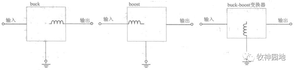
——According to the analysis just now, the input or output terminal is connected Inductors, then the input and output return grounds must not be connected in series with switch tubes or diodes, then the switch tubes and diodes can only be connected in series with the output/input and ground terminals respectively; and except for the power topology of BUCK and BOOST, we After combining the circuit, other topologies are invalid; for example, in the BUCK topology in the above figure: if the diode is connected in series to the input terminal and the switch tube is connected in series to the ground terminal, then when the switch tube is turned on, the input terminal and the ground terminal terminal short, not a valid topology.
The volt-second law is in the steady state of the power supply In order to work, all switching topologies must satisfy the law. If the volt-second law is not satisfied in the steady state of the power supply: Von * ton = Voff * toff; then we can get LΔIon ≠ L from the inductor formula VΔt = LΔI em>ΔIoff, then the magnetic field strength of the inductor core will be biased in one direction, which will eventually lead to saturation of the inductor core and damage the switch tube or the inductor itself.
Similarly, we have the same definition for the duty cycle of different switching topologies: the "on" time Ton of the switch tube accounts for the ratio of the switching period T, that is, D = Ton/T; if for the continuous mode T= Ton+Toff (in discontinuous mode: T > Ton+Toff). As shown in the figure below, we can derive the DC transfer functions of different topologies according to the volt-second law and the definition of duty cycle.
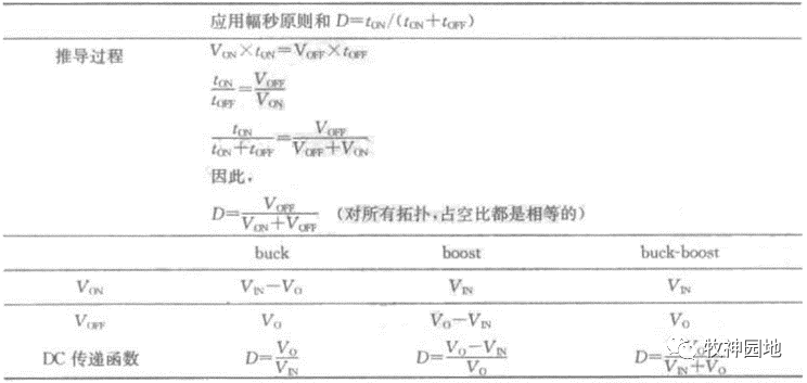
So we get the ideal case respectively (not counting Switch tube, diode, inductor, etc.) DC transfer function of three basic power supply topologies:
——We use the DC transfer function to see that when the input voltage of Vin is constant in all topologies, the duty cycle D becomes larger as the output voltage of Vo increases; but BOOST and BUCK- The maximum duty cycle of the BOOST topology cannot exceed 50%.
So what is the use of the DC transfer function of the switching power supply topology? We will break it down in detail in the specific design of the subsequent switching power supply.
The relationship between the various currents of the three basic topologies is shown in the figure below: IL is the average inductor current , Io is the output current, IIN is the input current, ISW is the switch tube current, and ID is the diode current.
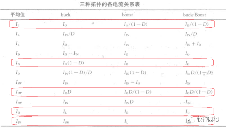
Regarding the relationship between IL and Io, it is important to note that :
For the BUCK topology, the inductor current IL is the same as the output current Io, because the inductor is connected in series at the output end, and all output currents flow through the inductor to provide;
< li>For BOOST and BUCK-BOOST topologies, the inductor current IL is not the same as the output current Io, even much larger than the output current (depending on its topology), which requires the inductors in BOOST and BUCK-BOOST topologies Larger volume.
DC transfer function of BUCK topology: D = Vo/Vin;
DC transfer function of BOOST topology: D = (Vo-Vin)/Vo = 1 – Vin/Vo;
DC transfer function of BUCK-BOOST topology: D = Vo/(Vin+Vo) = 1 – Vin/(Vin+Vo).
If the inductor is connected to the ground, a BUCK-BOOST topology circuit is obtained.
If the inductor is connected to the output, Then get the BUCK topology circuit;
If the inductor is connected to the input terminal, then get the BOOST topology circuit;
Surge current may be generated at the moment of contact between two signal lines, causing damage to the device. Pay attention to surge protection in the design.
li>
Similarly, we can analyze the requirements for each device from the relationship between the obtained switch current ISW, diode current ID, input current IIN, and output current Io.