-
Mail us
contact@tiger-transformer.com -
Phone us
(+86)15655168738
Mail us
contact@tiger-transformer.comPhone us
(+86)15655168738First, let’s talk about what crosstalk is. Crosstalk is two traces on a PCB. When they are not in contact with each other, one side interferes with the other, or interferes with each other.
The main manifestation is that the waveform has abnormal clutter, which affects signal integrity (SI) and so on. Generally speaking, it can be divided into two types: capacitive crosstalk and inductive crosstalk.

Capacitive crosstalk, as above As shown in the figure:
Two parallel traces in PCB can be equivalent to a capacitor. Of course, the capacitance of this capacitor is very small. Although it is very small, it is sometimes enough to affect signal integrity.
When there is high-speed signal transmission in one of the traces, this equivalent capacitor is constantly charging and discharging. The characteristic of the capacitor is to pass AC resistance DC, and the high-speed signal will be coupled to the other trace through the capacitor. Reducing signal integrity.
If the two traces in the above figure are located on adjacent upper and lower layers and are very close to each other, the equivalent capacitance will be larger and the capacitive crosstalk will be more serious.
Perceptual crosstalk, as shown in the picture above:

There are two parallel traces in the PCB. When one of the traces has high-speed signal transmission, an alternating magnetic field is generated. After this alternating magnetic field acts on the other trace, it will Induced current is generated inside the traces. The principle is similar to a transformer. Capacitive crosstalk and inductive crosstalk exist at the same time.
Nowadays, electronic products are becoming more and more integrated, the packages are getting smaller and smaller, and the wiring is getting denser and denser. Crosstalk is inevitable and cannot be eliminated. It should be reduced as much as possible, as long as the product is stable and reliable. . Here are several ways to reduce crosstalk:
1. Sensitive signal lines, such as audio and other analog signals, should be kept as far away from digital signal lines as possible.
2. Sensitive lines are strictly prohibited from running in parallel with digital signal lines.
3. The key high-speed signal lines should be wrapped with GND as much as possible, in a three-dimensional shape up, down, left, and right. GND can absorb various crosstalk noises and nip interference sources in the cradle. After GND wrapping, it basically meets the 3W rule.
For example:
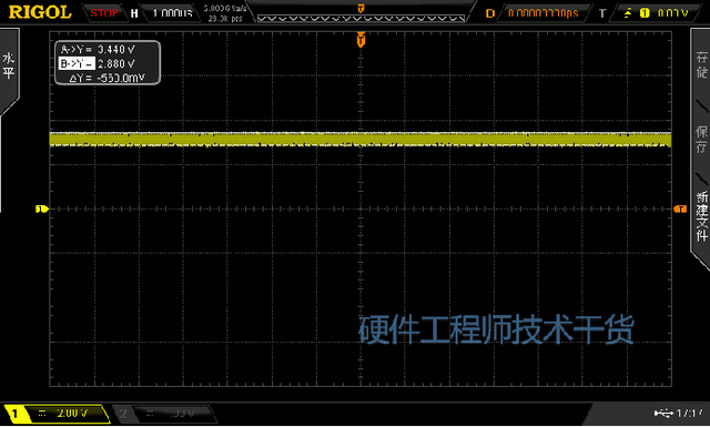
When doing board-level testing on a certain product of our company, we found that a certain GPIO waveform was abnormal, as shown in the figure below. The intuitive feeling is: the high level is very "thick".

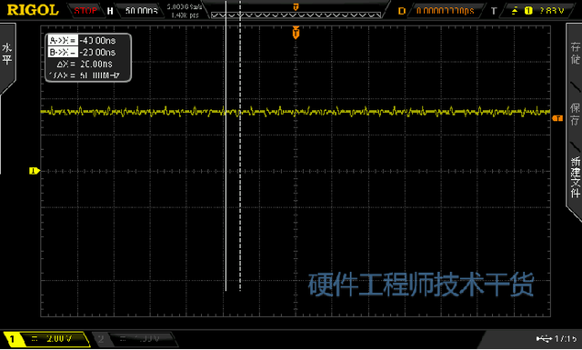
The waveform shown on the oscilloscope is like this, tens of MHz High-frequency signal, as shown below:

After looking at the circuit, I found that This GPIO goes a long way in parallel with a 25MHz CLK.
